Atotech (focusing on process chemicals, equipment, software and services) and ESI (focusing on laser drilling systems), both strategic brands of MKS Inc., the world's leading advanced technology supplier, will showcase their latest leading solut...
Atotech (focusing on process chemicals, equipment, software and services) and ESI (focusing on laser drilling systems), both strategic brands of MKS Inc., the world's leading advanced technology supplier, will showcase their latest leading solutions in the field of printed circuit board (PCB) and packaging substrate manufacturing at the 26th TPCA exhibition to be held at Taipei Nangang Exhibition Hall from October 22 to 24, 2025.
Ato Technology, a subsidiary of MKS, is strengthening its leadership position in promoting the next generation of advanced electronic technologies. By integrating cutting-edge technologies - including laser drilling, precision chemistry, electroplating equipment and process innovation - the company continues to advance its proprietary "Optimized Interconnect Technology" strategy. This strategy is designed to meet the growing demands for miniaturization, sophistication and performance improvements in printed circuit board and packaging substrate manufacturing.
With its commitment to innovation in the Asia-Pacific region and the global market, Ato Technology is deepening its cooperation with top manufacturers to promote the popularization and application of breakthrough technologies. These partnerships are critical to address the industry's drive for smaller structure sizes and higher reliability.
By integrating ESI's laser drilling systems with Ato Technology Electroplating's advanced chemical processes and electroplating equipment, the company provides comprehensive solutions to help customers meet the evolving challenges in the electronics manufacturing field.
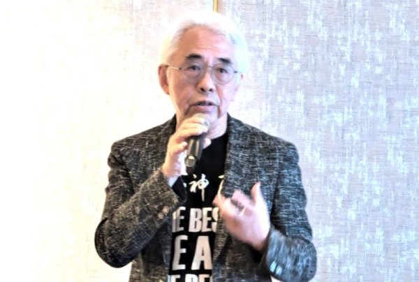
"MKS not only supports innovation, it drives innovation. Our integrated technologies are shaping the future of electronics manufacturing." said Dave Henry, executive vice president and general manager of global strategic marketing.
In 2025, ATO Technology will continue to invest in cutting-edge equipment and process technology through the Asia-Pacific Technology Center to promote the development of advanced electronic manufacturing. These upgrades shorten the development cycle of next-generation packaging carrier boards and support high-end SAP applications requiring line pitch and pitch of ≤ 5/5 micron.
The company's integrated solutions combine optimized laser drilling, electroplating and surface process chemistry with advanced manufacturing equipment to provide one-stop services covering pre-processing, via formation, electroplating and final surface treatment. This seamless integration enables customers to increase throughput, productivity and product performance without interrupting production processes.
ATO Technology Department is working closely with industry partners to jointly promote micro surface treatment technology (mSAP) for carrier board-level PCBs. By integrating the ESI and Atotech business units, we are launching sustainable solutions that are in line with the global CO2 emission reduction roadmap and environmental goals.
"Our focus is on driving innovation while supporting the industry's transition to a more sustainable manufacturing model," said Harald Ahnert, vice president and general manager of Material Solutions Chemistry.
"As the electronics industry continues to evolve, the demand for advanced carrier boards and sustainable manufacturing solutions is accelerating," said Wayne Cole, senior vice president of global sales and services. "Ato Technology is proud to promote this transformation by providing integrated technologies to accelerate the innovation cycle, improve accuracy and reduce environmental impact. At the TPCA exhibition booth N-620, Ato Technology and ESI experts will explain on-site how to help customers meet the challenges of next-generation electronics manufacturing."
In the chemical field, highlights of surface treatment include EcoFlash® S300, a differential etching solution for advanced packaging carriers, and Novabond® PX-S2, a high-tech inner layer adhesion promoter designed for high-speed AI applications. In the field of metallization, highlights this year include the Printoganth® MV TP3 process, which enables ultra-thin copper deposition with fine line widths up to 2/2 micron line width and spacing, and works best when paired with the revolutionary copper-based activation system Cupraganth® MV. In the field of electrolytic copper plating, the company focuses on promoting the advanced copper filling process InPro® Pulse TGV suitable for high aspect ratio through-glass through-holes, and the mass-production proven Cuprapulse® XP7 UA precision bonding plating solution, specially designed for the new generation of packaging carrier boards. Final plating solutions include: Aurotech® G-Bond 3, a universal gold solution suitable for nickel/gold, nickel/palladium/gold and palladium/gold plating; Stannatech® 2100, an economical final plating solution with excellent solderability and corrosion resistance; and PD Core®, a low metal content electroless palladium plating solution suitable for ENEPIG and EPAG processes.
PCB equipment system promotion projects include: G-Plate® - a new generation of high-capacity tools dedicated to the through-hole plating process of packaging carrier boards, achieving the highest yield and cutting-edge thin line capabilities, with a target line width/space of less than 5/5 microns; vPlate® is an advanced HDI The vertical continuous plating equipment designed with the packaging carrier board has the industry's top surface uniformity; last but not least is the new Uniplate®, which is the company's flagship high-capacity system and industry-leading horizontal plating equipment, specially designed for the next generation of HDI PCB and packaging carrier board manufacturing.
The promotion focus of laser drilling equipment includes: the latest Capstone™ system, which achieves high-efficiency/high-throughput breakthrough productivity in flexible PCB UV drilling; and the Geode™ series (carbon dioxide and UV laser solutions suitable for HDI and packaging carrier boards). Special highlights of the exhibition: Geode™ A - a new carbon dioxide laser system, specially designed for high-precision and high-speed ABF laminate processing; Geode™ G2 - a new carbon dioxide laser system, achieving high-precision and high-speed HDI and micro surface mount board (mSAP) through-hole drilling. The Geode™ platform offers 15% higher optical transmittance, 21% smaller total service area, and up to 65% lower energy consumption.
Daniel Schmidt, director of global marketing and training, said: "We are honored to continue to cooperate with IMPACT and host this year's IMPACT titled "Driving Artificial Intelligence and High-Performance Computing: A Turning Point in Advanced Packaging and Interconnect Technologies." Special session of industry forum. This session will focus on the innovative development of advanced artificial intelligence packaging technology, covering the transformation of organic substrates to glass cores, as well as cutting-edge PCB process solutions designed to meet the evolving needs of artificial intelligence chip and packaging substrate manufacturing. 》
This year, Ato Technology and ESI not only sponsored and participated in the well-known IMPACT conference, but also joined the newly upgraded open seminar series "Tech x Total Technology Solution Trend Conference". Two of the keynote speeches will be presented by the Taiwan STT team and the equipment team. The presentation will be held in N-1131 on the fourth floor of the Nangang Exhibition Hall..
A4 / B5 sessions Session/Time Topic speaker A4 session: 10/22, 16:00~16:40 Exploration of thin line circuit formation technology in advanced packaging Shang Yujie Senior Product Marketing Manager B5 session: 10/23, 16:00~16:40 Closed-loop IIoT platform for smart, lean and sustainable PCB manufacturing Qiu Haozhi Equipment manager IMPACT MKS ATO Technology Industry Forum speakers, location and timeTopic: Driving Artificial Intelligence and High-Performance Computing: A Turning Point for Advanced Packaging and Interconnect Technologies
date location time Topic speaker 10/22 Tuesday R504b 13:00-13:20 Future of AI hardware enabled by advanced packaging Daniel Ng Technical lead and AMD fellow, AMD 13:20-13:40 Advanced Packaging: unleashing the true potential of semiconductor chips Bora Baloglu Business Development Director, Intel 13:40-14:00 Next generation IC substrates to address emerging challenges Venkata Mokkapati Business Development Director, AT&S 14:00-14:15 Advancing Redistribution Layer Plating for enhanced Reliability and Performance Christian Ohde General Manager, MKS’ Atotech 14:15-14:30 Silicon to PCB key Technology inflections impacting advanced packaging Kuldip Johal CTO, MKS’ Atotech 14:30-15:00 Panel Discussion Host by Daniel Schmidt & Eddy Chen Marketing Director & Manager, MKS’ Atotech IMPACT MKS ATO Technology and ESI Technology Forum Speakers, Location and Time date location time Topic speaker 10/21 Tuesday R502 16:00-16:15 Innovative Electrolytic Flash Copper Plating Equipment for Enhanced mSAP Via Reliability and Efficiency Tobias Sponholz MKS’ Atotech General Manager BU PP 17:00-17:15 Laser Trenching (LLV) – Leveraging AODs for quality and productivity Chris Ryder MKS’ ESI Sr. Director Business Development 17:15-17:30 A Modular Electroless Copper Bath System for SAP Applications Laurence Gregoriades MKS’ Atotech Sr. Manager R&D PTH 10/22 Wednesday R502 10:40-10:55 Integrated Beam Characterization and Z-Axis Control for Enhanced Laser Focus in FPCB Via Drilling Joe Hasty MKS’ ESI Sr. Manager Engineering R504c 13:45-14:00 A next generation non etching adhesion promoter enabling streamlined process for Advanced IC substrates Thomas Thomas MKS’ Atotech Sr. Manager Marketing STT R504b 17:00-17:15 Tool-Agnostic Pulse Reverse Electroplating for High Aspect Ratio Through Glass Vias in Advanced Packaging Tobias Sponholz MKS’ Atotech General Manager BU PP 17:45-18:00 ADDRESSING NEXT-GENERATION IC SUBSTRATE CHALLENGES: MKS ADVANCED LASER DRILLING OF RESONAC MATERIAL FOR HIGH-DENSITY PACKAGING Weiming Cheng MKS’ ESI Sr. Mgr, Business Development R502 17:00-17:15 Closed-Loop IIoT Control for Sustainable and Intelligent PCB Manufacturing: A Data-Driven Approach Integrating Domain Expertise Giovanni Obino MKS’ Atotech Sr. Director, Industrial Digital SolutionsFor more information, please see: TPCA Show 2025