Japanese new semiconductor manufacturing company Rapidus published an article on its official website with the theme of "2-nanometer Semiconductor Challenge: Exploring Rapidus' Technical Breakthrough", detailing the necessity of 2-nano...

Japanese new semiconductor manufacturing company Rapidus published an article on its official website with the theme of "2-nanometer Semiconductor Challenge: Exploring Rapidus' Technical Breakthrough", detailing the necessity of 2-nanometer in the current technological society, as well as the progress of Rapidus' development in this field and its relationship with partners. Rapidus mentioned at the end of the article that with its profound technical strength and a strong alliance, Rapidus will surely become a new Japanese force in the global semiconductor elite.
Rapidus points out that semiconductors are the foundation of today's digital society, and it continues to evolve to provide faster speeds and stronger processing capabilities. The key driver behind these advances is circuit miniaturization, which means constantly shrinking the transistor size to accommodate more transistors on a single wafer. Today, the semiconductor industry is entering the 2nm (2nm) era, which is the most advanced technology to date.
In semiconductor manufacturing, the term "processing point" refers to the iterative substitution of manufacturing technology, usually in nanometers. The smaller the nanometers, the stronger the processing capacity and the ability to draw narrower circuits. Although these numbers have directly reflected the physical extreme length of the transistor in the past, modern structures have separated the node names from the actual size. Today, a date name like 2nm roughly reflects the progress of iteration, and usually each generation experiences a 0.7-fold microscopic trend. The mini-shrinkage of the day has a significant impact on performance, integration, cost and power efficiency. The smaller transistor shortens the propagation distance of the electron and speeds up the turn-off speed to improve computing performance. Higher transistor density allows each wafer to carry more functions, while increasing the number of wafers per wafer can reduce production costs. In addition, the reduced slash size reduces the charge required to turn on, thereby reducing power consumption, which is a key factor in the energy efficiency of battery-powered equipment and data centers.
Rapidus in the article supplements the micro-reduction of the process further improves the various phases of the semiconductor design, including performance, functionality, cost and power consumption. Because of this, companies around the world compete to develop smaller process stages, following Morrow's law, and progresses about every two years.
Rapidus said that Gordon Moore, who later became the founder of the Intel joint in 1965, proposed the theory that what was later called Moore's Law. He pointed out that every 18-24 months, the number of components (such as transistors) on the overall circuit doubles. This forecast has driven the rapid development of decades, and promoted the improvement of electronic product performance and cost reduction. However, as the technology approaches the 20nm node, the traditional planar transistors gradually increase in leakage current and current flow when the technology is turned off, becoming a significant problem. The velvet-style field-effect transistor (FinFET) launched in the early 2010s effectively suppresses leakage current by designing the trench into vertical tiles with three sides.
At the same time, the 193nm ArF excimer laser used for exposure is difficult to form a pattern below 10 nanometers, which leads to the development of transition technologies such as immersion incomplete exposure and multiple patterning. Finally, extremely ultraviolet (EUV) exposure technology was adopted, which makes patterning of 7 nanometers and below possible. Looking ahead, further miniaturization will not only rely on the minusculation of transistors, but also on the 3D integration, new materials, chips and new transistor architectures of the Postmore era.
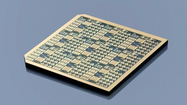
Rapidus emphasizes that 2-nanometer semiconductors are expected to bring significant improvements over early stages such as 7-nanometer and 5-nanometer. According to IBM's 2021 data on 2-nanometer prototype wafers, the performance of 2-nanometer wafers can be 45% higher and the power consumption can be reduced by 75% compared to 7-nanometer wafers. Although FinFETs can be extended to the 3nm era, they also face the limitations of increased leakage at smaller sizes, and GAA transistors should be born. They use nanosheets or nanowires as ducts and are completely engulfed, further improving control and suppressing leakage, making the transistor smaller in size while still achieving higher performance. IBM's prototype uses a three-layer silicon nanosheet GAA structure, which surpasses FinFETs in both performance and efficiency.
Based on the above situation, the 2nm node is particularly important for artificial intelligence and Internet of Things. Artificial intelligence workloads require extremely high computing performance and energy efficiency, so semiconductors that can meet these needs become key. While providing the required processing capabilities, the 2nm wafer is also energy efficient, making it an ideal choice for artificial intelligence servers and edge devices. For billions of small, usually battery-powered Internet equipment, 2nm technology allows advanced artificial intelligence to operate locally without consuming a lot of power.
However, 2 nanometers also bring great challenges. Variability and yield control have become more difficult, and the EUV exposure system price is extremely expensive, and only a few companies around the world can afford this level of production. However, even in the face of these challenges, 2 nanometers will still be the cornerstone of the next generation of digital-based facilities.
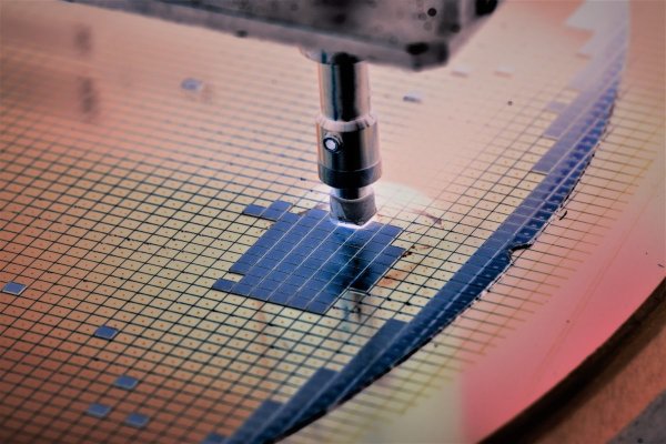
Rapidus further pointed out that in the fiercely competitive logical semiconductor market, global leaders such as Telco, Samsung, and Intel are taking the lead. Rapidus, based in Japan, was established in 2022 with the support of eight major Japanese companies and the support of the Japanese Ministry of Economic Industry (METI), with the goal of realizing 2-nanometer production in China in the late 2020s. Therefore, Rapidus is working with IBM to promote the 2-nanometer process. In 2023 and 2024, more than 150 engineers were sent to New York to receive next-generation process technology training. At present, about 80 engineers have returned to the Thousand Years’ Company to optimize the wafer prototype manufacturing process.
In April 2025, Rapidus started the trial production line at the 1000-year-old Innovative Manufacturing Integration (IIM-1) Grooving Factory in Hokkaido, planning to produce samples later that year and conduct mass production in 2027. Rapidus' new IIM-1 foundry factory represents a major improvement in the traditional foundry model, and also re-imagines how the crystal factory can think, learn, adjust and optimize the process through cutting-edge methods and technologies.
In addition, Rapidus is also working with Tenstorrent, an artificial intelligence computing company based in California, to jointly develop an artificial intelligence processor IP for edge applications. Global semiconductor leaders are increasingly interested in Rapidus' 2-nanometer technology. Rapidus is building a wide range of partnerships. In addition to IBM, its partners include nano-economic R&D center imec and a wide range of equipment and material manufacturers, which will have a place in an advanced biosystem centered in Hokkaido, along with Rapidus. In the future, with its profound technical strength and a strong alliance, Rapidus will surely become a new Japanese force in the global semiconductor elite.